

The Galaxy S20 Ultra is an impressive engineering marvel, and Samsung has managed to cram in a massive screen, huge camera sensors, the best connectivity features, and a massive 5000mAh battery inside a thin package. Now, iFixit has posted a teardown of the smartphone, offering us a detailed look at the phone’s internal parts and their assembly.
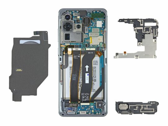
First and foremost, the phone’s glass and metal design are held together by glue, so one would require a heat gun to remove the back. The phone’s wireless charging coil can be seen on top of its truly massive, 5000mAh battery. Samsung has used only one type of Phillips screws inside the phone, which makes things a bit easier. After removing the charging coil, antennas, and speakers of the phone, the mainboard can be seen featuring camera sensors, mmWave hardware, and other essential parts of the phone.
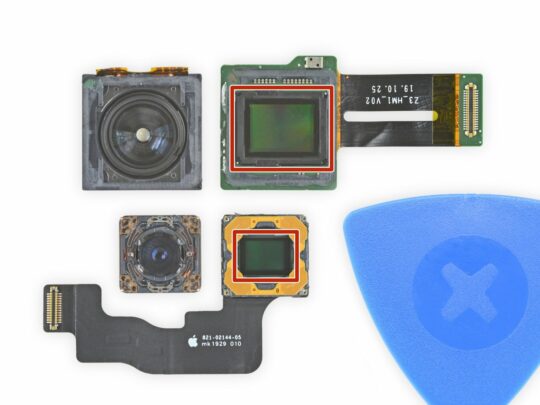
Next up, the 108MP ISOCELL Bright HMX camera sensor (1/1.33-inch). It is one of the largest smartphone camera sensors in the market, and it is twice the size of the primary camera sensor used in the iPhone 11 series. This sensor uses a 3×3 pixel binning method, which Samsung calls ‘nona-binning,’ to improve low-light image quality.
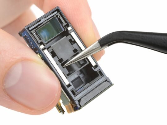
The teardown also offers a look at the marvelous periscope 4x optical zoom mechanism sitting. To fit such a complex zoom lens mechanism into a phone that’s just 8.8mm thin, the company has used a prism to bounce the light at a 90-degree angle in front of the 48MP Sony IMX586 sensor. It appears that Samsung has used multiple levels of hardware stabilization to reduce the shakes.
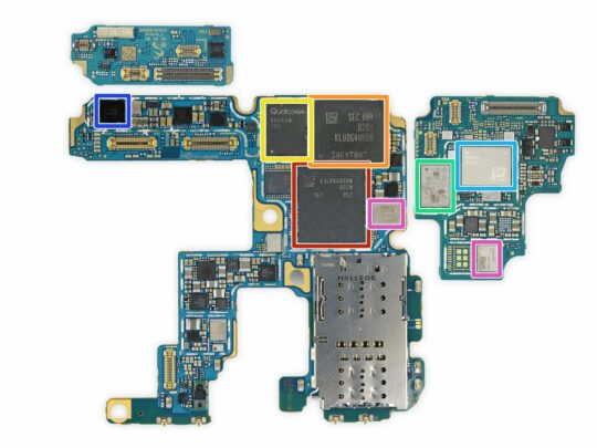
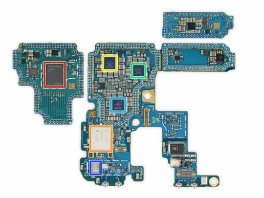
The phone’s mainboard also features the Snapdragon 865 processor with the Samsung 12GB LPDDR5 RAM layered over it. There’s also 128GB of UFS 3.0 storage, Qualcomm’s second-gen 5G modem and 5G amplification modules, a power management IC from Maxim, and a couple of RF front-end modules from Skyworks and Qorvo.
Flipping over the mainboard reveals even more chipsets. There’s a Bluetooth and Wi-Fi module from Murata along with three power management ICs, an RF transceiver, and a front-end module from Qualcomm. There are a lot of Qualcomm chips in there. We wonder if the Exynos variant of the phone also features as many Qualcomm chips.
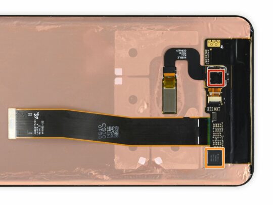
The Galaxy S20 Ultra’s 5000mAh battery is glued to the phone’s frame and removing reveals a mmWave antenna. Removing the big, 6.9-inch Super AMOLED screen reveals a 3D Sonic fingerprint sensor from Qualcomm and a display driver that makes the 120Hz refresh rate possible. iFixit notes that the phone’s internal parts are laid pretty much the same way as the Galaxy Note 10+ 5G.
iFixit has given the Galaxy S20 Ultra a low repairability score of 3 out on a scale of 10 owing to a lot of glue and the display repair requiring a complete teardown of the phone or replacing half the device.
The post Galaxy S20 Ultra teardown offers a detailed look at phone’s internals appeared first on SamMobile.
from SamMobile https://ift.tt/3arsoUd
via IFTTT


ليست هناك تعليقات:
إرسال تعليق